The story so far: On July 15, the Union Cabinet cleared the second phase of the India Semiconductor Mission (ISM), and the Mobile Phone Manufacturing Scheme (MPMS), with a ₹1.27 lakh crore and ₹62,500 crore outlay, respectively.
The programmes are aimed at encouraging the next cohort of semiconductor fabrication, assembly, and packaging facilities in India, as well as following through on encouraging more phone assembly and component manufacturing in the country.
The government expects the scheme to draw ₹4 lakh crore in investment, ₹2 lakh crore in production, and ₹1 lakh crore in exports over its tenure of five years.
How is this different from the first phase?
ISM’s first phase was approved in December 2021 with an outlay of ₹76,000 crore.
Following an amendment in 2022, the programme was empowered to provide for up to 50% capital subsidy for big-ticket projects, such as Micron’s memory chip packaging facility in Sanand, Gujarat.
The funds were also directed to the Electronics Component Manufacturing Scheme, which was designed to incentivise additional manufacturing of smaller electronics components.
The Gazette notification laying out the precise details of the second phase is set to be published by next month.
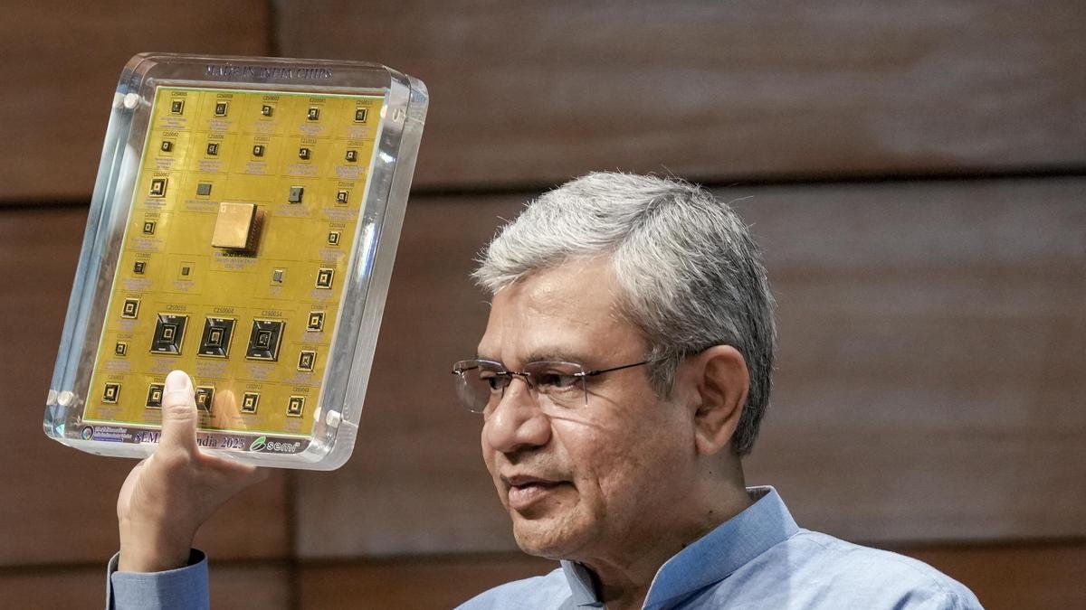
In the meantime, Information Technology Minister Ashwini Vaishnaw and Ministry of Electronics and Information Technology (MeitY) Additional Secretary Amitesh Kumar Sinha have offered a few details of the expanded scope of the programme.
The main change is that the ISM programme will now cover a larger part of the electronics manufacturing ecosystem, including areas that were partially addressed in the previous phase.
These include encouraging chip design talent, capital machinery (the large equipment used in chip-making facilities), chemicals and gases that are of semiconductor-grade purity, and research and development efforts.
The newer scheme will also trim capital subsidies to 30-40%, Mr.
Sinha said, as the semiconductor industry is likely to get more attractive in India even with less incentives.
The government is also less likely to offer land support, as State governments have shown increasing enthusiasm for hosting such projects by providing land at token prices and offering their own incentives on top of those provided by the Union government.
India’s semiconductor push will create countless jobs: PM What have been the outcomes of phase 1?
Of the 12 manufacturing and packaging units approved in phase 1, with a total committed investment of ₹1.64 lakh crore, most are semiconductor packaging units.
Nine such units are spread across Gujarat, Uttar Pradesh, Punjab, Assam, Odisha, and Andhra Pradesh.
In addition, there is a silicon fabrication unit, and one gallium-nitride Micro LED display fabrication unit.
The Tata Electronics fab is set to start commercial production in 2028.
The scheme included a design-linked incentive programme, under which 24 projects have been approved.
The government has also obtained licences for expensive semiconductor design software and provided them free of cost to universities and startups.
The Semiconductor Lab, Mohali, which is being revamped, is being positioned as a facility to help “tape out” chips designed by students and researchers.
Why is India focusing on semiconductor manufacturing?
From the COVID-19 era supply chain disruptions to export controls initiated by the U.S. during the trade war with China, there has been a growing sense that India needs to integrate more tightly with global electronics value chains.
The government has insisted that building domestic capacities is essential even if it takes decades to reach the level of countries, such as the Netherlands and Taiwan, whose companies are critical in chipmaking.
India’s old computing wars offer a roadmap for future chips How sophisticated are the chips targeted in the current facilities?
While the most powerful phones use “frontier” grade chips, with a process node of 7 nanometres or even less, the Union government has targeted 28nm chips (which are made in what are called “legacy” process nodes).
There is a massive market for these chips, Mr.
Vaishnaw reasoned, as everyday electronics, where size and computing power are not constraints, require such components too.
As ISM 2.0 progresses, the government hopes that the ecosystem will progress to frontier nodes, especially by improving the level of domestically owned intellectual property and research for such chips.
While semiconductor designers are aplenty in India, most work for either foreign firms or on their behalf, leaving royalties and expertise outside the domestic industry.
Why is MPMS being notified?
While a growing share of iPhone sales around the world come from handsets assembled in India, most components remain imported, and there are barely any Indian-designed handsets in the market.
The MPMS aims to incentivise both the expansion of domestic phone assembly as a way to grow the ancillary market, and to incentivise domestic design and research and development.
To that end, the scheme provides for incentives ranging from 2.25% to 5%, depending on the level of local design involved in the handsets.