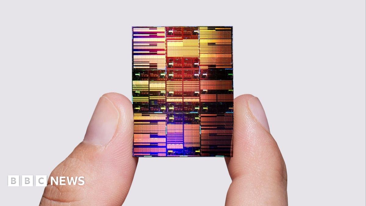
IBM on Thursday unveiled what it claims is the world’s first technology capable of producing semiconductor chips smaller than one nanometre, marking a significant breakthrough in the race to develop more powerful processors for increasingly demanding AI workloads.
The announcement comes as chipmakers search for new ways to sustain the decades-long trend of packing greater computing power into ever-smaller spaces, a principle commonly associated with Moore’s Law.
As artificial intelligence drives demand for faster and more efficient chips, breakthroughs in advanced semiconductor manufacturing are becoming increasingly critical to the industry’s future.
What Makes IBM’s New Chip Technology Significant?
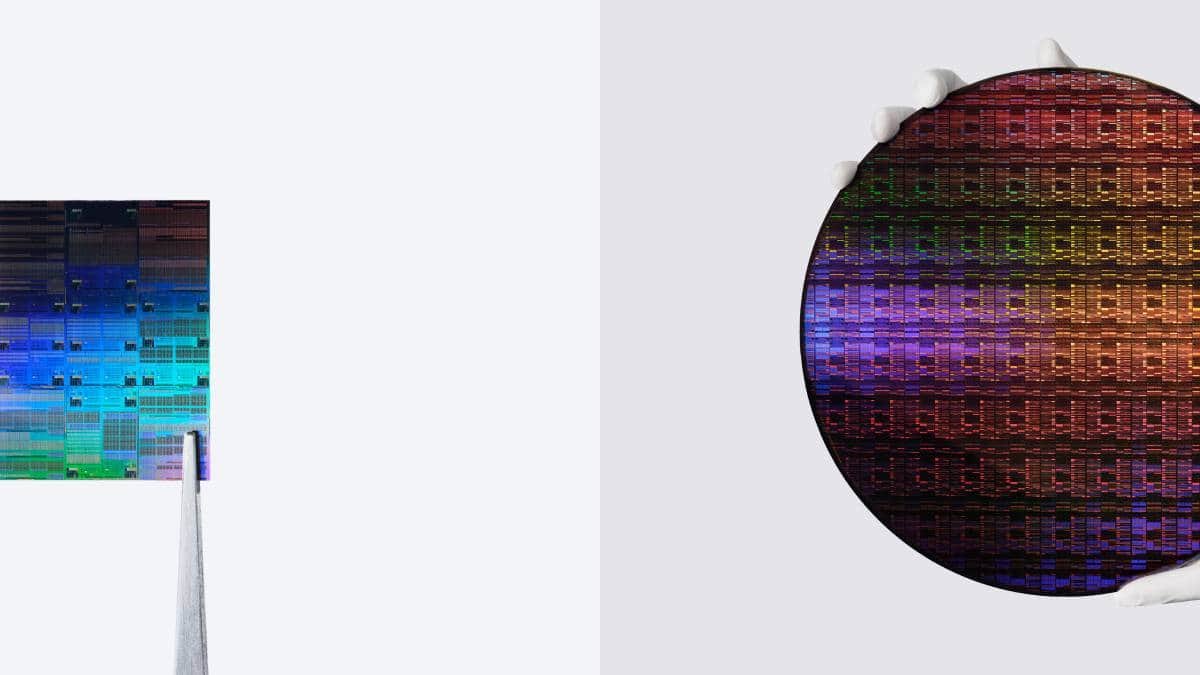
At the heart of IBM’s breakthrough is a new three-dimensional transistor architecture called Nanostack, which the company says is the industry’s first nanosheet-based design capable of enabling chip production below the 1-nanometre threshold.
The technology allows transistors to be stacked vertically, dramatically increasing transistor density while improving performance and energy efficiency.
According to the company, the technology could deliver up to 50% higher performance or 70% better energy efficiency compared to current-generation 2nm chips.
More from Tech Elon Musk backs Andrej Karpathy amid Claude tag backlash, calls for X algorithm overhaul ‘Saved so many lives’: Did Google really send alerts moments before earthquakes hit Venezuela?
The architecture also allows different materials to be used across stacked transistor layers, enabling engineers to independently optimise each layer for speed, power consumption and efficiency.
IBM says this could be particularly valuable for compute-intensive applications such as generative AI, cloud computing, advanced smartphones and next-generation data centres.
Another key milestone is the extension of semiconductor scaling beyond the nanometre era and into the angstrom scale, where chip features approach atomic dimensions.
IBM’s 0.7nm technology, equivalent to 7 angstroms, demonstrates that further miniaturisation remains possible despite concerns that Moore’s Law was approaching its physical limits.
While the technology is still in the research stage, IBM expects the earliest commercial adoption of its Nanostack architecture within the next five years, potentially laying the groundwork for a new generation of AI-focused processors and high-performance computing systems.